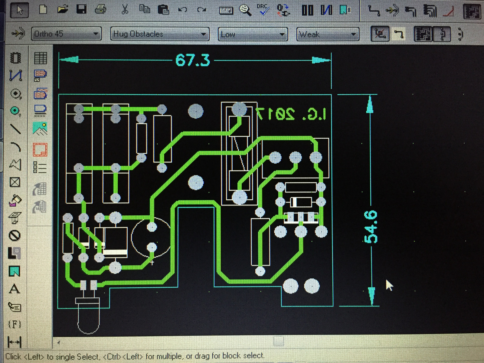
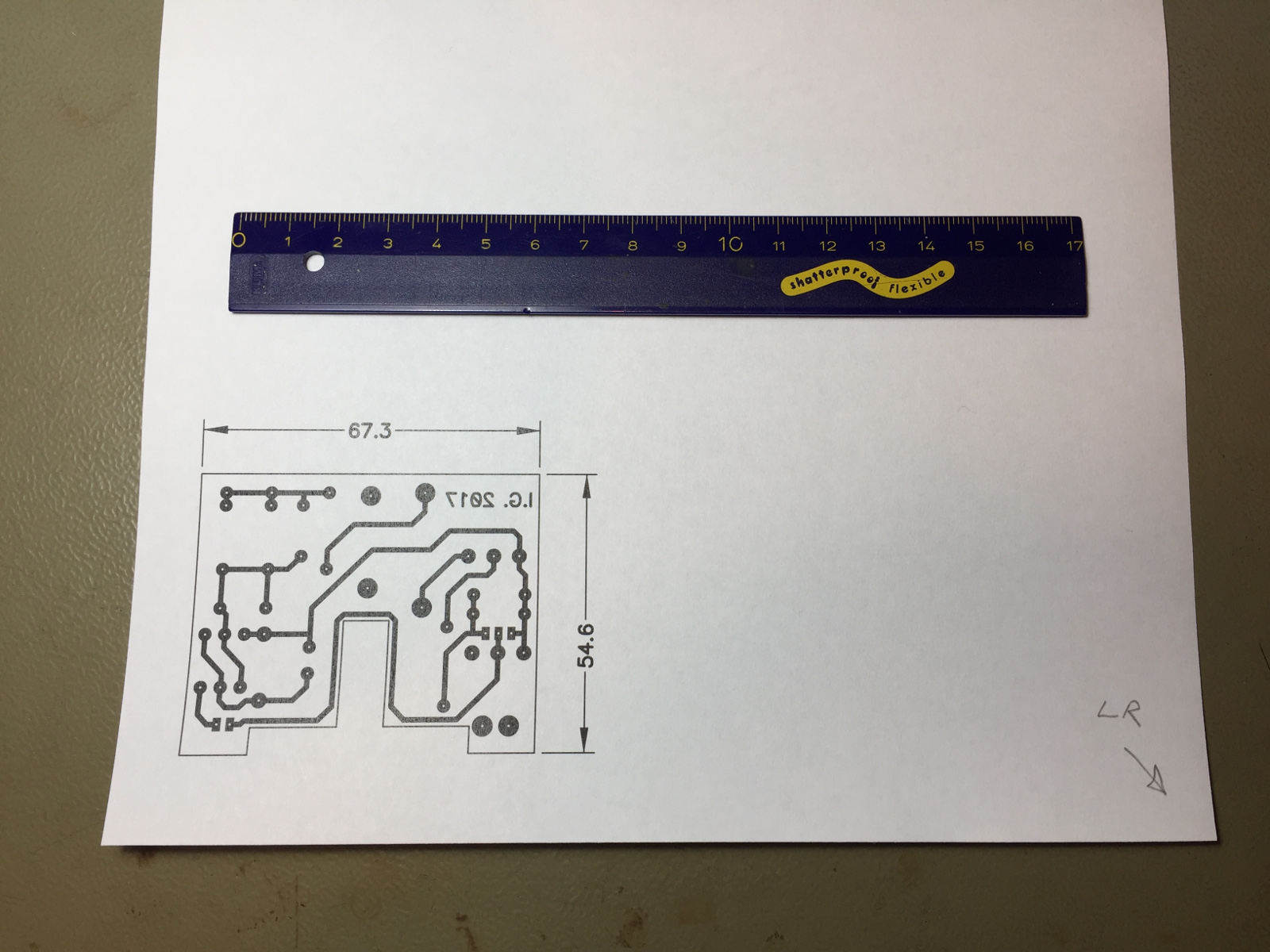
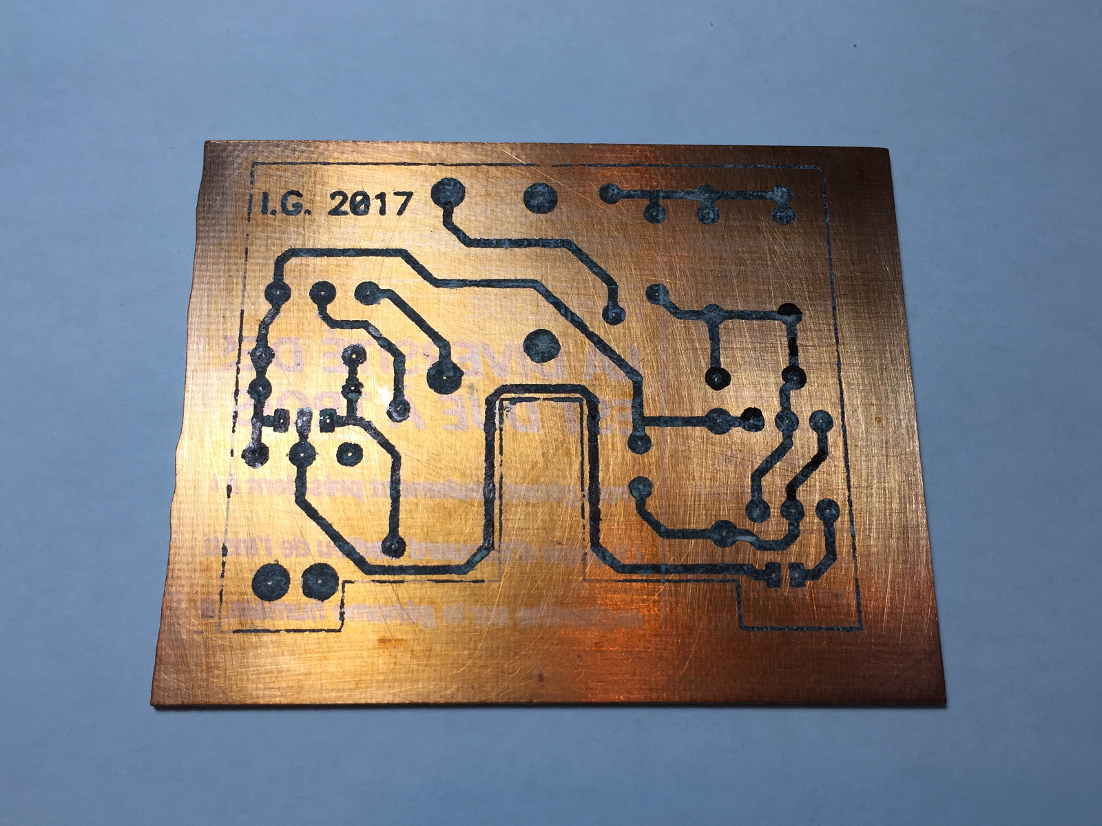
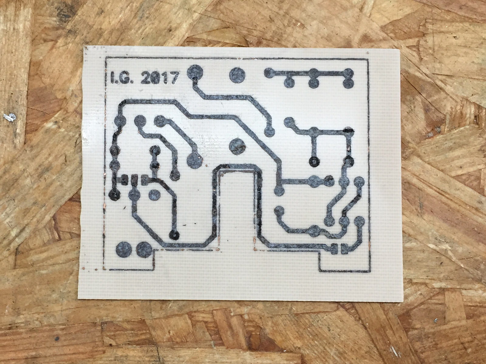
The PCB design is done and it's ready to be printed. I always include some text to make sure I won't accidentally create a mirror image. (click to enlarge).
Etching a printed circuit boards (PCB) at home is a need that every electronic homebrewer has, almost every time he thinks about building a circuit. Of course, there are plenty of techniques that do not require etching, like using protoboards, wire wrapping, dead-bug style and many others. These techniques may be excellent for the desired application, but in some cases, a true etched PCB is a must. For example when you need several identical circuits, when you need a precise track geometry for very high frequency applications, when you want a beautiful and good looking circuit, when you need to use small surface mount components (SMD) or in many other cases, there is nothing like a true etched PCB. Etching PCBs at home is not very difficult and requires very little (and cheap) equipment, but it's extremely time consuming.
Assuming you already have a design, maybe created with some CAD software, printed on a magazine or even hand drawn on a piece of paper, there are basically three steps to get a finished PCB: first you need to transfer your design on the copper, then you need to etch the copper and finally you need to do some mechanical work like drilling or cutting. There are several options for each step and some of them are discussed hereafter. Of course, my preferred methods are explained in details.
The PCB design is done and it's ready to be printed.
I always include some text to make sure I won't accidentally create a mirror
image. (click to enlarge).
Ok, you want to make your own PCB: start by buying some copper-clad boards, one or two-sided according to your needs. The most common substrate is FR-4 (which is made of glass fiber and epoxy), 1.6 mm (1/16") thick with one or two copper layers of 35 μm (1.4 mils): this will be fine for the vast majority of home projects. There are other board thicknesses if you're concerned by weight or mechanical strength. There are thicker and thinner copper layers if your have to run high currents or are concerned by costs of the copper. There are also special substrate materials that perform well with microwaves or that are flexible, but the standard FR-4/1.6mm/35μm really fits almost any normal application.
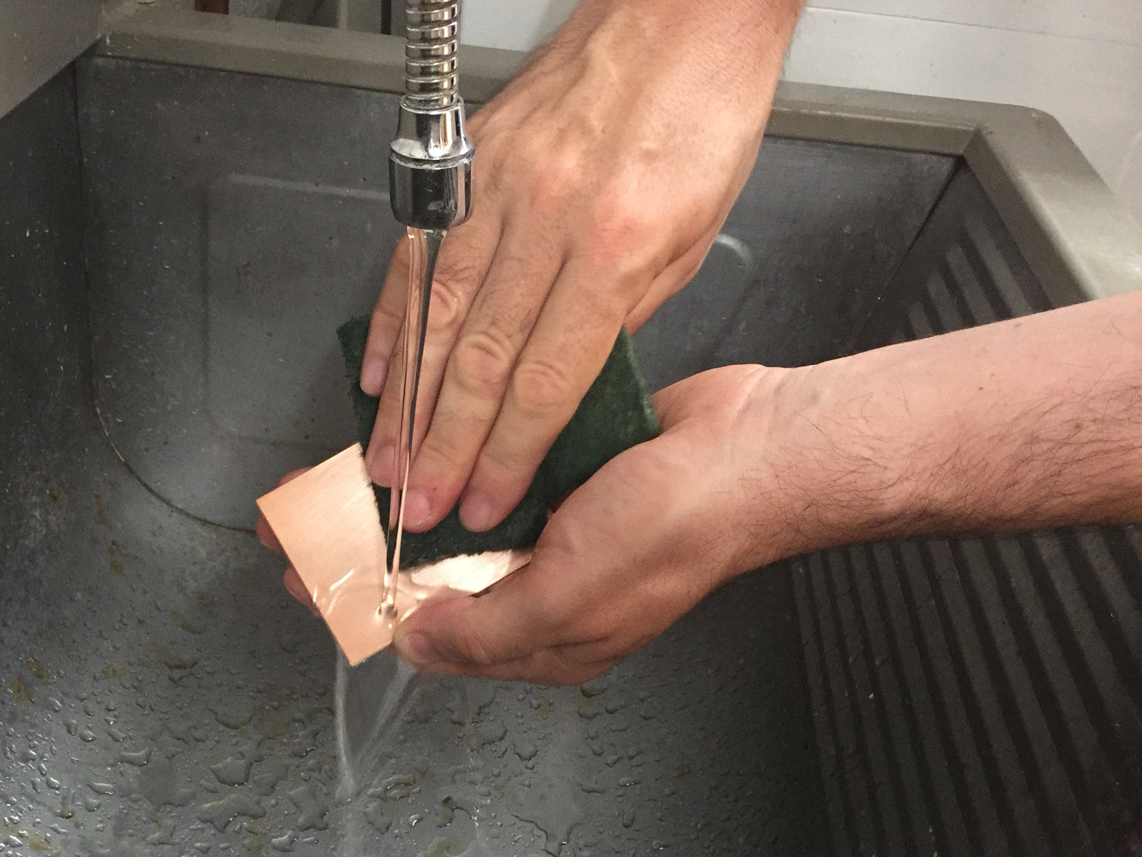
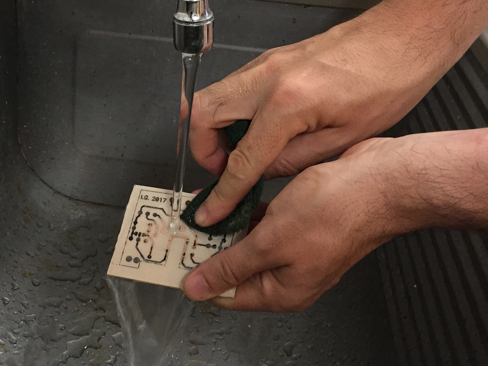
Cleaning the PCB with an abrasive pad, some soap and water.
(click to enlarge).
Unless you're using boards with a photo-sensitive varnish already on (see-below), you want to start by cleaning the copper surface(s). Any dirt, oxidation, grease or fingerprints will disturb the etching process and you'll probably end up with unwanted copper spots on your final PCB: they don't look good and may short your traces together. So use an abrasive sponge with some dish soap and rub the surface meticulously: the copper has to be shiny and red. Than wash it to remove all the soap and let it dry. From now on, don't touch the copper with your fingers anymore; use gloves or touch only the edges.
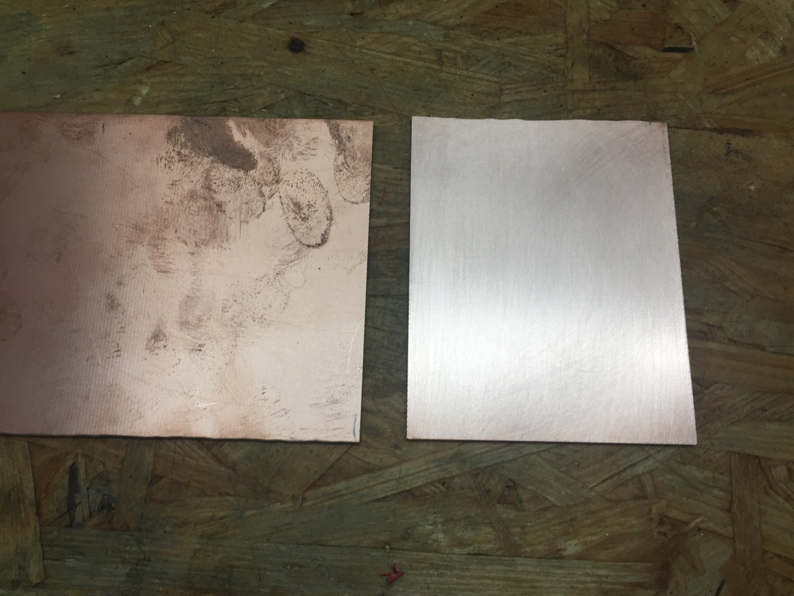
The PCB on the left has not been cleaned yet, the one on the right is
good for transferring the layout.
Please remark how shiny the copper surface is and how all traces of grease
and oxidation have been removed. (click to enlarge).
Look at the difference in the above picture: you want a nice, shiny and uniform copper surface, no oxidation and no grease.
The first problem you have to face is how to transfer your design to the copper: of you don't have CAD software and need only one PCB, you can use the old method of direct drawing. Use a permanent marker and draw your traces directly on the copper. One layer of ink is not enough, let it dry for 10 minutes and redraw it again on top to make the layer thicker. Two layers are the strict minimum, three is safer. If the ink is too thin, the etchant will eat the copper underneath. If you make a mistake, you can scratch off the extra ink with a dull knife.
These two PCBs have been hand drawn, and letter transfer has been used only
for the pads of the DIL ICs.
The traces of the one on the left have been tinned with solder, mainly for
esthetic reasons. (click to enlarge).
Instead of a permanent marker you can also use nail polish: one layer is usually enough, but it's much more expensive. For complicated and precise patterns like IC footprints, you can use letter transfer. This also works for adding text or drawing straight traces. And you can combine all these methods on the same PCB.
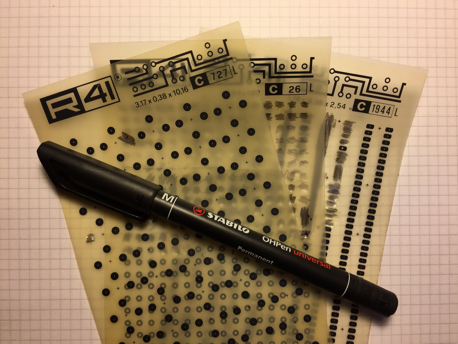
Picture of some (old) letter transfer sheets and a permanent marker (click to enlarge).
Even if this method works and I've used it for a long time, it's extremely time consuming, it makes only one PCB and the result looks hand drawn.
A very good but complicated method is photo-transfer. For this, you need to apply a thin and uniform layer of photoresist varnish on your copper (or buy PCBs with photoresist already on), print (or photocopy) your layout on transparent films, lay the film on the PCB and expose to UV light in a contact copier for a precise amount of time, than develop the exposed varnish in a developing bath. It's very similar to analog photography and fun to do, but requires chemicals and an UV contact copier. Applying a uniform layer of photoresist is not easy and you have to work fast (or in low light conditions). You can buy PCBs with photoresist, but they are expensive. Exposure time is quite critical and you have to do several trials every time you change photoresist or transparent film. Finally a contact copier is also expensive, especially a double sided one, even if you build your own.
One common problem with this method is that the black ink on the transparent film can be not black enough resulting in slightly exposing the traces. One solution is to print the layout several times on top of each other by putting the film again in the printer. This will increase the thickness of the ink, but alignment is critical and it's not easy to do. Using a different printer or film material is usually a better option.
After using this method for many years, I decided to look for a simpler method.
Toner transfer is in my opinion the simplest and most effective way of transferring a PCB layout to the copper. You just need a PC, a laser printer, some glossy paper and a flatiron: chances are that you already have them all on hand. The idea is to print a mirror image of your layout on the glossy paper, than transfer the toner to the copper by reheating it with the flatiron. For this, you really need a laser printer; an inkjet printer won't work.
I use thin glossy paper from fashion magazines: you don't need fresh white paper, as the print on the magazine won't mix with the toner, but I prefer pages where there is only thin text on white background on both sides: avoid parts where there are large printed areas like images or huge letters. What's already printed on the page will not disturb the toner, but later it will prevent water from soaking the paper that will be hard to peel off.
You can also buy special toner transfer paper and gives slightly better quality, but glossy magazine paper works well and it's much cheaper. If you're not satisfied with the results you're having, try a different magazine.
Don't touch the paper with your fingers: you don't want grease on the surface. Use a brand new magazine, wear gloves or touch only the borders.
Test print on a blank A4 sheet.
The hand-drawn arrow on the right helps placing the paper in the correct way
in the printer tray; the ruler is to check that the scale is exactly 1:1; the
text on the PCB should appear as mirrored. (click to enlarge).
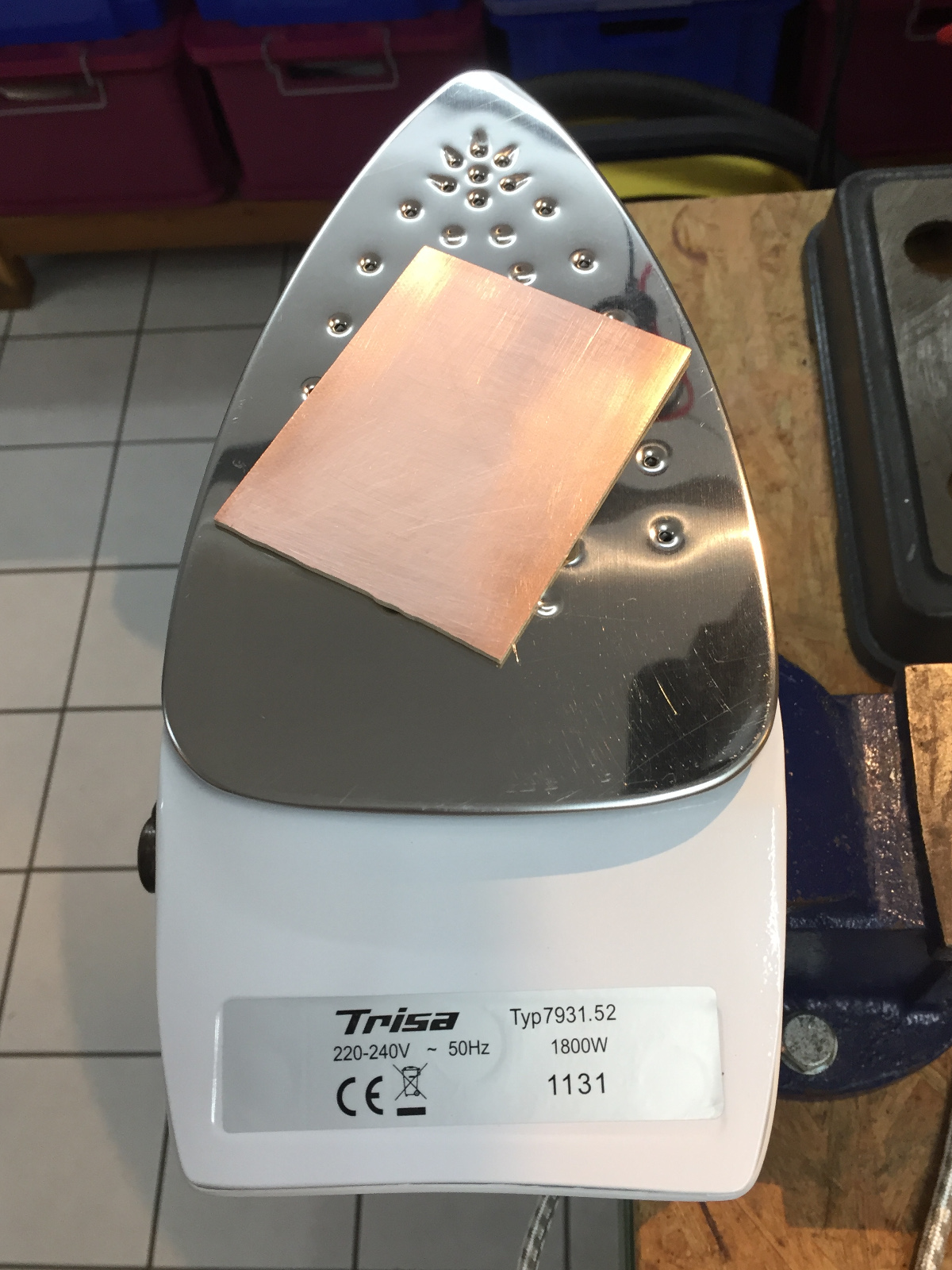
I start by printing the layout on normal paper to see where it is printed on the page and how big it is, than I glue a piece of glossy paper on a blank new page, put in the laser printer and print it again.
Don't forget to print a mirror image of what you need: when you will transfer the toner, the image will reverse. It's a good practice to always add some text on the PCB that should be read by watching the copper, so that you won't accidentally etch a mirror image of your circuit... because it's a mistake that is very easy to make.
The glossy paper has been glued to a new blank A4 paper with just two
points of glue. (click to enlarge).
Use just two little spots of paper glue. Do not use adhesive tape, as it will melt with the heat of the laser printing process. Do not glue all four corners; the glue may break when the paper bends on the internal rollers of the printer and you'll end up with a jam in your printer. I use a "roller" type of non-permanent paper glue, but a stick of paper glue will work just as well. You only need a tiny amount. Apply glue outside the useful area of your layout.
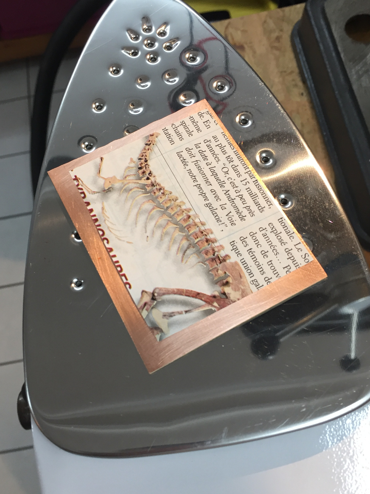
After printing the PCB traces, it will look like this.
No worries: toner and glossy paper prints don't mix. (click to enlarge).
Now heat the flatiron to a medium temperature, you'll need a little more than 200 °C. Preheat the PCB on the iron for a few seconds, than lay the printed glossy paper on the copper (toner against the copper) and apply a uniform pressure. The glossy paper will stick to the copper. To avoid the glossy paper to stick to the flatiron, use a piece of photocopier paper in-between.
Preheating the PCB on a flatiron. (click to enlarge).
Be careful not to get burned: the flatiron is hot and the PCB can get quite hot as well. Wear heat resistant gloves like the ones you use in the kitchen. Rather than hand holding the flatiron (as it's intended to be used), I usually hold it upside-down in a vise, so that resembles a "hot plate" and I can simply lay the PCB on the hot surface. This will keep both your hands free.
Application of the glossy paper with the toner (face down) on the hot PCB. (click to enlarge).
I use a small block of wood to apply a uniform pressure on the glossy paper. Wood is a good thermal insulator and will not transfer the heat of the flatiron to your fingers. Still, be careful.
Be careful: paper, wood, gloves and other materials are flammable. Do not leave them on the iron for too long. Keep a fire extinguisher on hand, just in case.
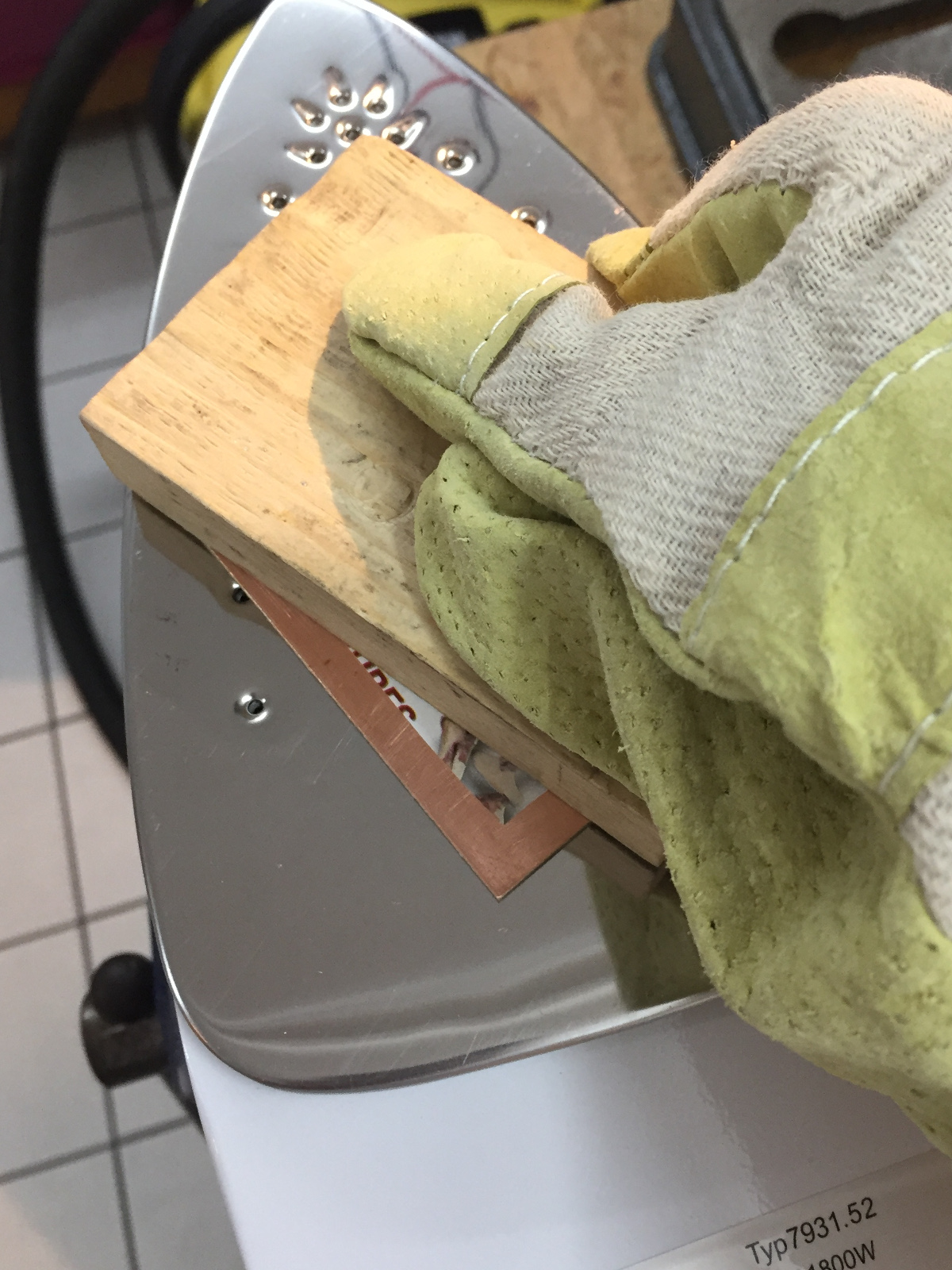
Appling pressure through a block of wood to make the toner adhere to
the copper. (click to enlarge).
If you have a laminating machine, use it to apply a uniform pressure. Usually these machines aren't hot enough to melt the toner, but you can use the flatiron to heat up the PCB/glossy paper and quickly insert them in the laminating machine for applying a good pressure. If you don't have one, you can still get away with just a flatiron, but requires some more practice.
I modified my laminating machine by replacing the thermal switches to increase its temperature. Still, it's still a bit on the cold side and I need a flatiron anyway. To prevent it from overheating, I cut off the top part of the cover. This also allows better handling of the PCB.
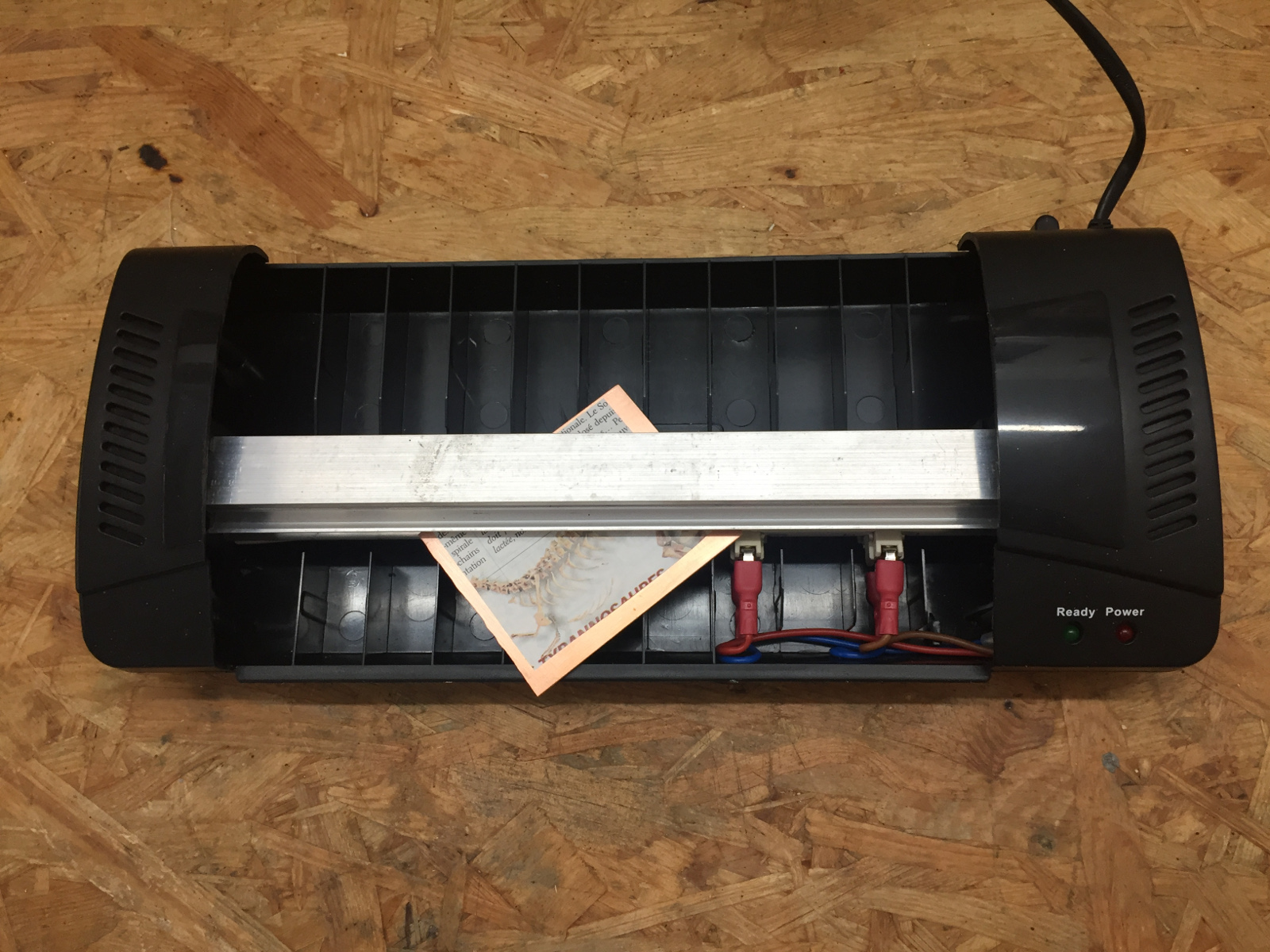
Using a (modified) laminating machine to apply uniform pressure on the
whole surface.
Several passes are necessary. (click to enlarge).
Once the toner has been transferred (it's now sticking to both the copper and the paper), it's time to remove the paper. Don't peel it off yet: you will destroy the layout. For this, first soak the paper in some warm soapy water.
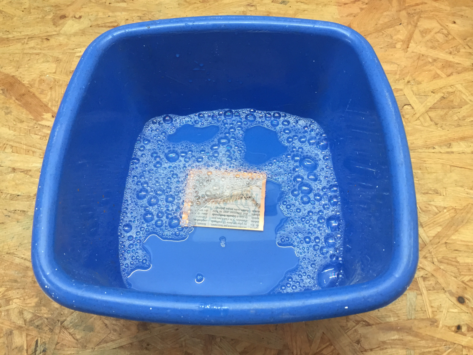
Soaking the glossy paper with warm soapy water. (click to enlarge).
Apply pressure repeatedly with your finger as if the paper was a sponge: this will make it absorb more water. Let it soak for a few minutes, then gently peel off the paper; the toner should stay on the copper and the paper should come off in one piece.
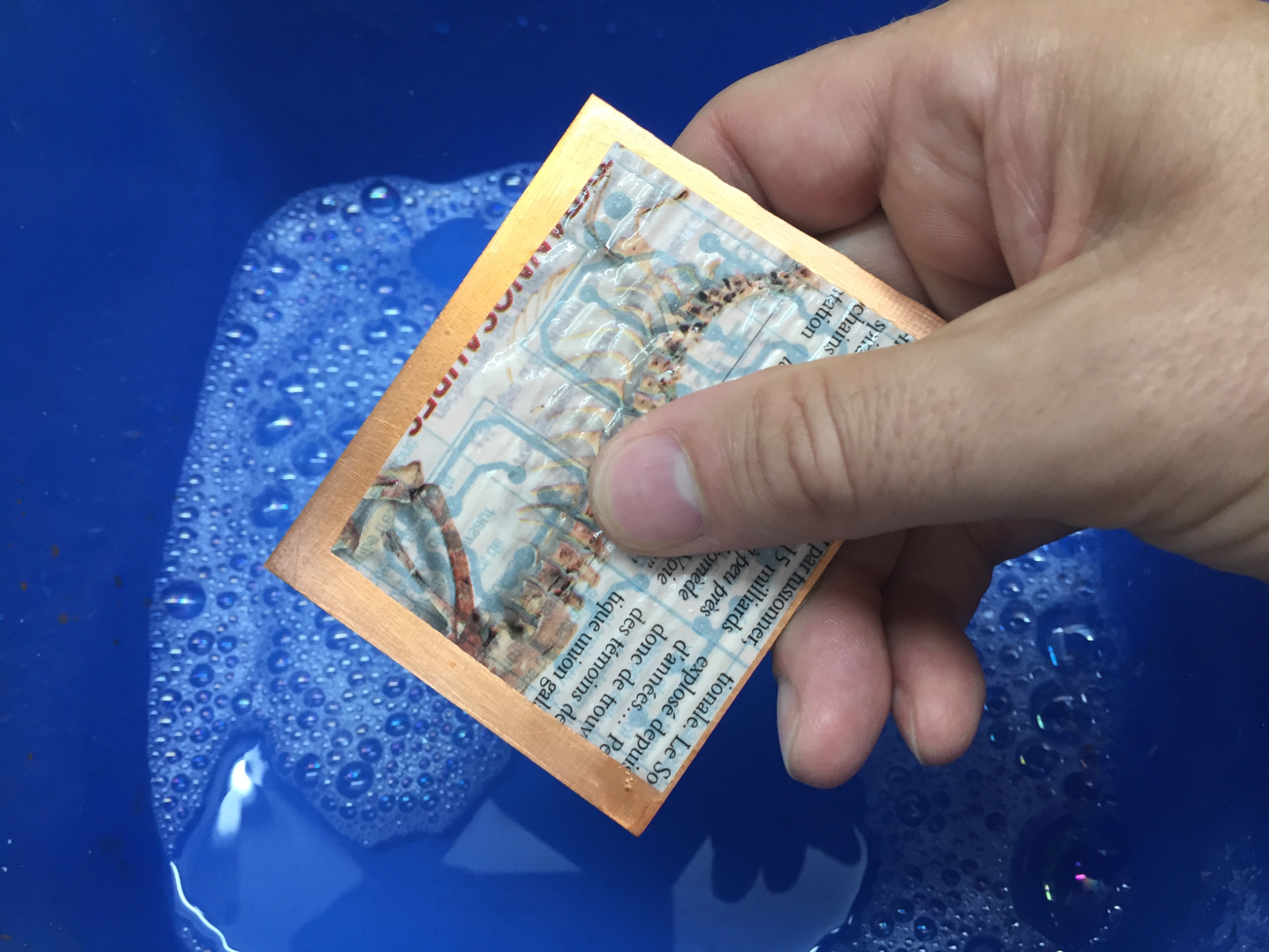
Applying some pressure on the paper with the fingers to make it soak
more water. (click to enlarge).
The paper should peel off easily, in one piece. If it stays stuck to the PCB, it didn't soak enough or you didn't apply enough pressure with your fingers.
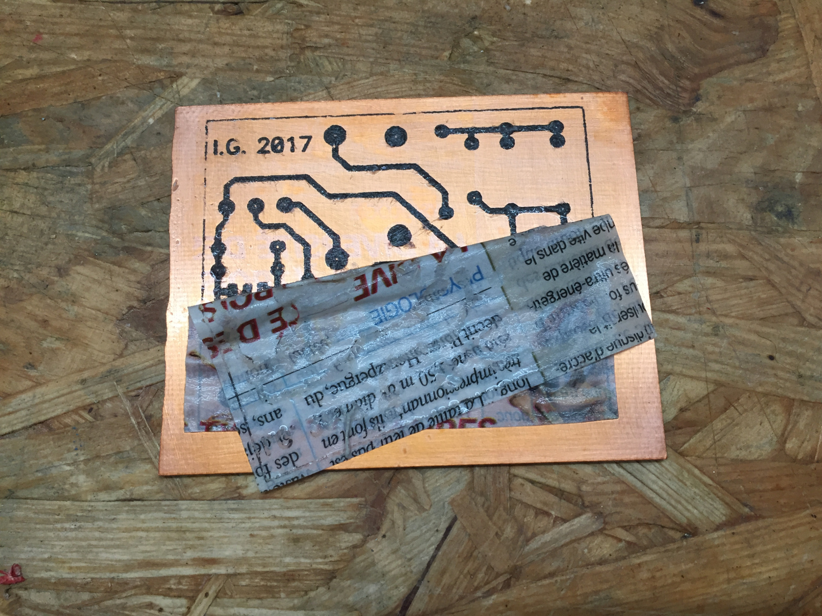
Peeling off the glossy paper.
The toner is transferred to the copper.
Note that the text is now readable. (click to enlarge).
Wash it, let it dry and inspect the result. You will notice, as it dries, that some paper fibers are still stuck to the toner and it becomes light gray instead of black: this is ok as long as the toner is uniform and there are no fibers between the tracks. Remember not to touch the copper with your fingers.
Not all toner transferred well, so I had to re-touch some areas with a
permanent marker.
Now the PCB is ready for etching. (click to enlarge).
If you're happy with the result, you're ready to etch. If not, you can still retouch it a little bit by scratching unwanted parts with a dull knife or by adding missing parts with a permanent marker. If you're not happy enough, you can still remove all the toner by scrubbing with the abrasive sponge and start again; after all, at this point you've only lost a piece of glossy paper.
Once you have transferred your (positive) design on the copper, i.e. you have a protective layer on the metal you want to keep, you are ready to etch. There are several ways to do it, the most common for home use being ferric chloride, but here I want to explain an alternative and faster method.
Usually to etch the copper from the PCB, an aqueous solution of ferric chloride (also called iron(III) chloride, FeCl3) is used. It works quite well but it's terribly slow: a fresh solution will probably etch a PCB in about 30 minutes. But as copper is consumed from the boards, the etchant becomes saturated and less effective: the time required can easily double after a few PCBs. Furthermore, the speed of this reaction is also dependent on temperature, the colder the slower. Since I do my etching outside (to avoid breathing the fumes), in winter I sometimes had to wait more than three hours for a PCB.
Stirring the liquid will speed up the process; heating it up and bubbling in some air will help as well. Some people use aquarium equipment to automate these three actions.
Ferric chloride is a dark brown liquid that will stain almost anything it touches, so cleaning and maintaining the equipment is a very delicate and unpleasant job.
During the etching you have to look after your PCB: if you leave it to long in the solution, tracks and pads will start to be etched as well. And if you leave it way too long, all the copper will disappear! So you have to check the status periodically to see when it's ready.
I should also mention sodium persulfate (Na2S2O8) as classic way of etching PCB. Its use and performance are very similar to ferric chloride, but it's a transparent liquid that becomes more and more green with usage. It has the advantage that you can see your PCB being etched. It doesn't stain as bad as ferric chloride but it's still very aggressive and will damage the majority of materials it's spilled on, especially your clothes.
I had enough of waiting for the ferric chloride to do its job and I was looking for alternatives. One day, a friend of mine told me his own recipe based on hydrochloric acid and hydrogen peroxide: it's cheap, the chemicals are easy to find and it can etch a PCB in about 30 seconds! Yes, 30 seconds, really.
This method uses some pretty aggressive chemicals and it's an extremely good idea to wear safety equipment: you don't want this stuff to touch your skin, your eyes, your clothes or anything else. So, always wear safety gloves and safety glasses. Keep fresh water on hand to wash out any spill.
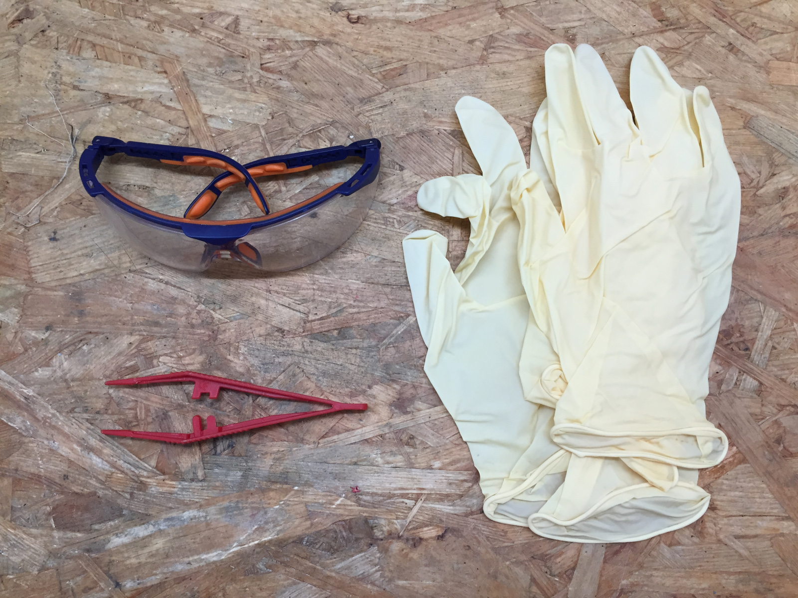
Safety gear: protective goggles, plastic tweezers and plastic gloves.
(click to enlarge).
During the etching, the reaction is quite violent; a lot of bubbles are released and tiny droplets spill all around. You don't want to breathe the fumes, so always work outside in a ventilated area and don't keep your face too close. Wear a mask. Please also keep in mind that this stuff will attack many metals like stainless steel: beware of nearby objects, like a stainless steel sink, a chromed faucet or your wristwatch.
To handle the PCB in the solution I use plastic tweezers so that I don't have to dip my fingers in the acid. Even if I always were gloves, I prefer to keep my fingers at a safe distance.
First, you'll need the following chemicals:
Hydrochloric acid and hydrogen peroxide are easily available in hardware stores: look for cleaning and pool care products. They are quite cheap and with 1 liter of each you will be able to etch plenty of PCBs. For example, for a board of 10 × 4 cm2 you'll need about 10 ml of each.
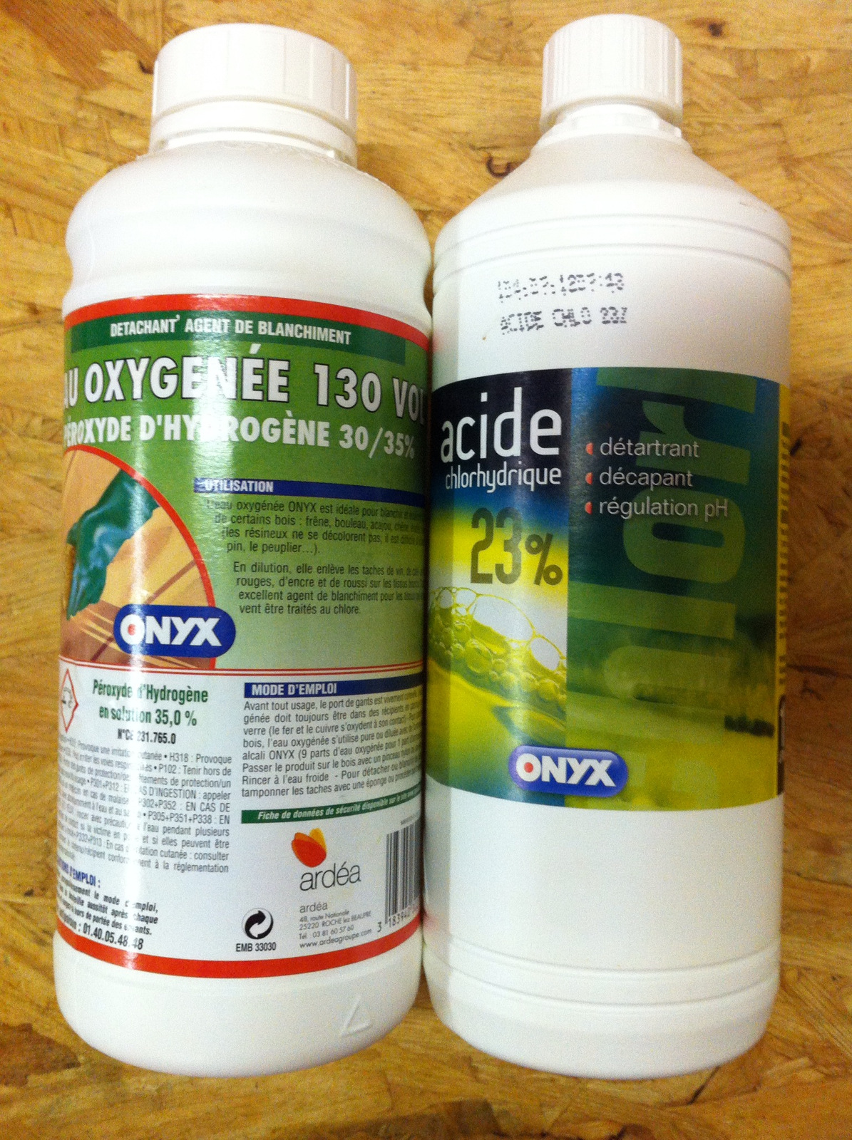
Hydrochloric acid and hydrogen peroxide (click to enlarge).
Again, those chemicals at those concentrations are aggressive: wear safety gear.
The etching solution can be used only once and must be prepared right before the etching process. To minimize waste, use a plastic tray that will just fit the PCB you want to etch. For small boards I often use empty plastic boxes used to sell nuts or machine screws.
If you're using a new tray, you may need to know how much solution is required to cover the board: I use the syringe with plain water to measure how many milliliters I need, then I empty the tray before using the real etching solution.
To prepare the solution, start by pouring with the syringe 1/3 of the required volume with water directly in the tray. I use regular tap water, but if you encounter any problem, using distilled water is a good idea. Then, with the syringe add another 1/3 of the final volume of 23% hydrochloric acid. After rinsing the syringe with fresh water I add the last 1/3 of 35% hydrogen peroxide. Always recap the bottles of chemicals immediately to avoid breathing the fumes and also because the peroxide spontaneously decomposes to oxygen and water if left open.
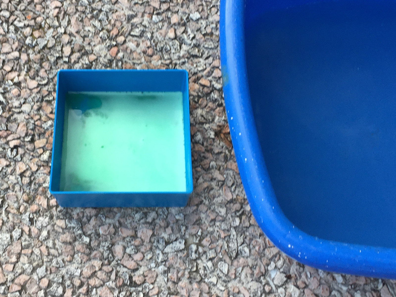
The copper is being etched in the hydrochloric acid and hydrogen
peroxide solution. (click to enlarge).
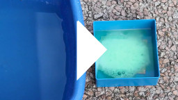
This mixture will only last e few minutes, so you have to start the etching quickly. Simply put the PCB in the solution, copper side up, push it to the bottom with a plastic tool and watch. For double sided PCBs, you need to add plastic spacers between the PCB and the tray so that the solution can get to the bottom side.
Watch the movie of the etching with hydrochloric acid and hydrogen peroxide,
in real time: pcb-etching-video.mp4
(8,976,701 bytes, 1:33, H264, 854 × 480, 23 fps).
The reaction is almost immediate, quite violent and exothermic. The liquid starts to bubble and becomes green. The reaction slows down after about 30 seconds when all the visible copper is etched and the PCB is ready. Take the PCB out of the solution and rinse it with tap water. Be careful because the solution is now quite hot. Beware also because the reaction slows down but doesn't stop: if not removed, all the copper on the board will disappear in a few minutes.
You can only etch one PCB with the etching solution: if you try to etch a second one right after the first, the solution being hot and therefore more performant, the second PCB may disappear in a few seconds. If you wait for the solution to cool down in-between, the accelerating effect of the peroxide will disappear and the second PCB may take several hours to complete. It's best to dispose of the used solution and prepare a fresh one for each PCB.
The etched PCB. (click to enlarge).
Once the etching is done, all copper between the traces is gone, but you still have to remove the toner that is on the traces. This can be easily done by rubbing the PCB with an abrasive pad and some water.
Removing the toner after etching: again just some scrubbing with an
abrasive pad and some soapy water. (click to enlarge).
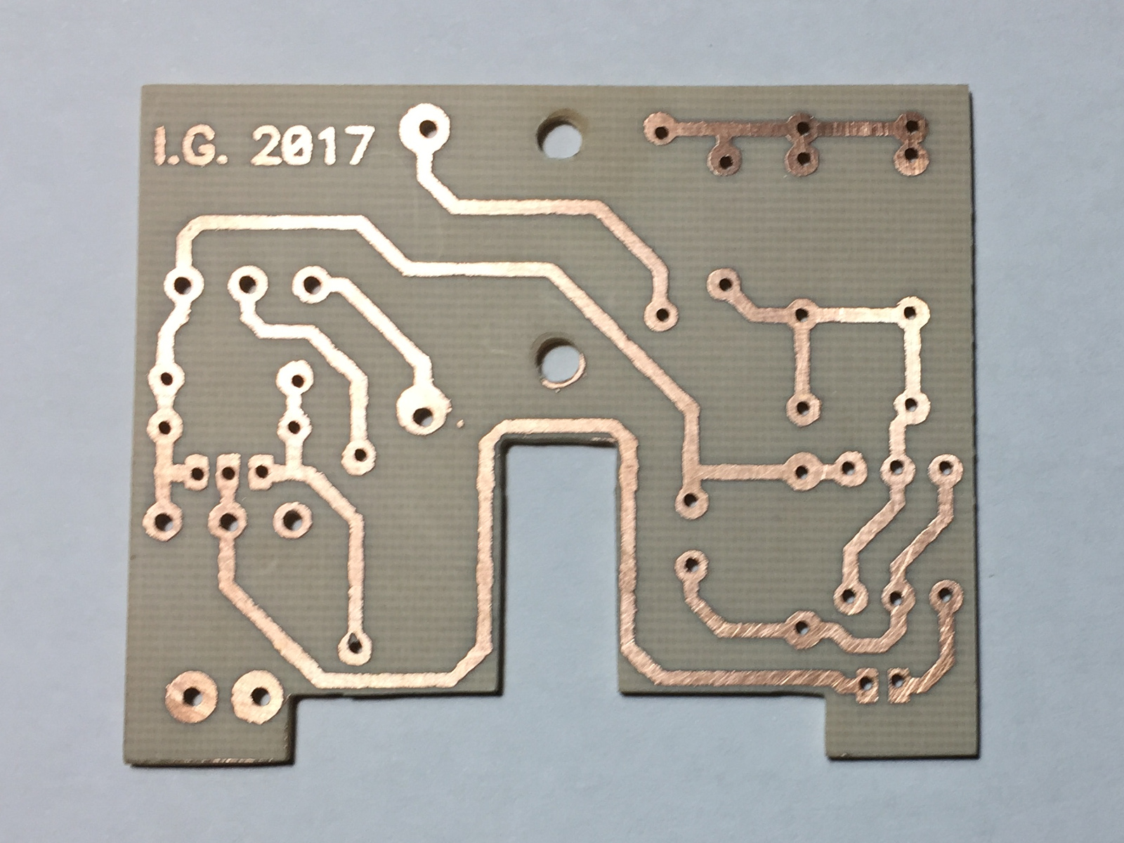
The picture below shows the result of the etching process: a nice and shiny PCB ready to be drilled and cut to size.
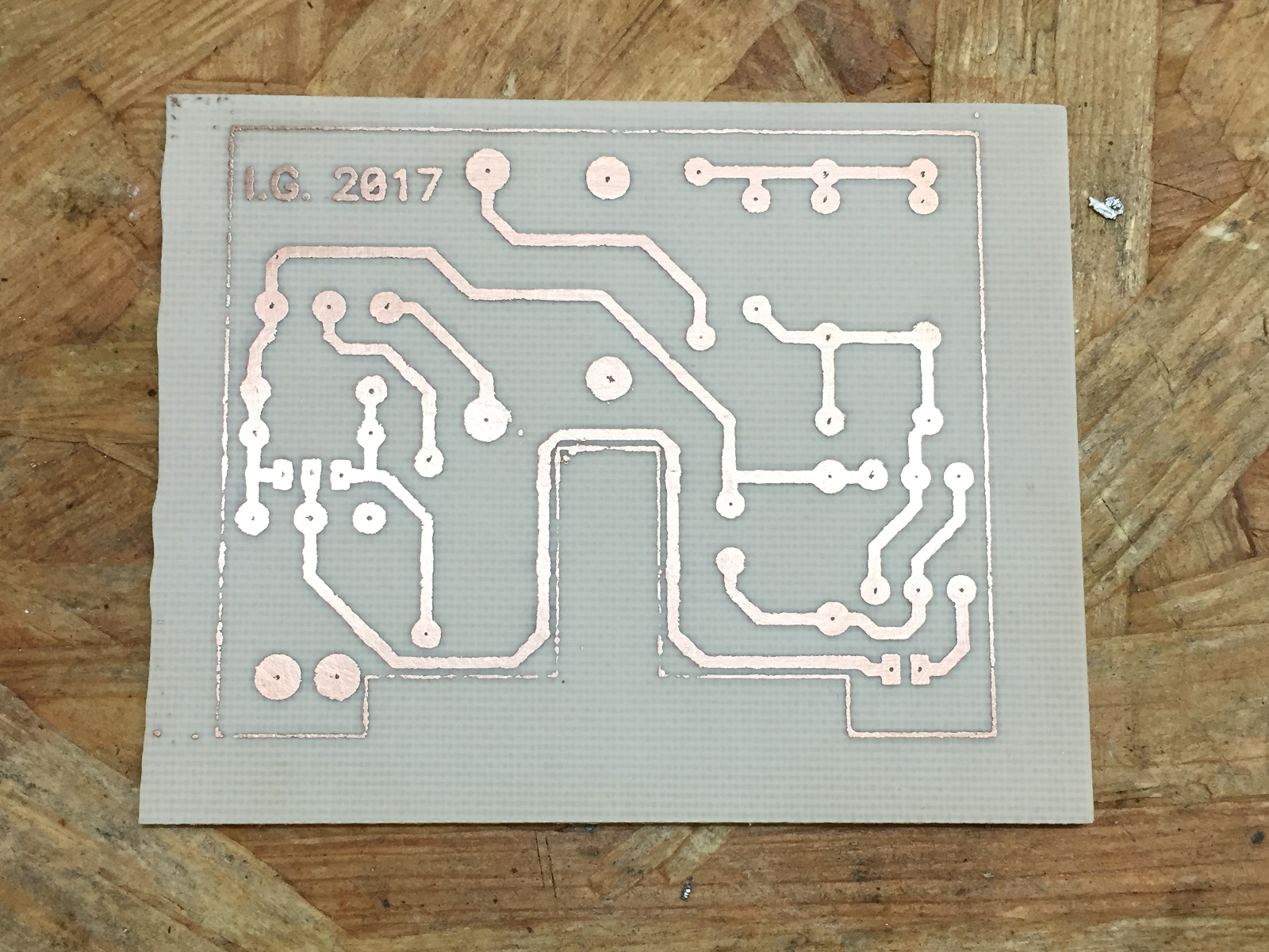
The copper traces after removing the toner. (click to enlarge).
For disposing the solution after the etching process, I store it in a sealed container, I label it "HCl + H2O2 + Cu" so that I know what's inside and bring it to the collection center where I put it with used paints and solvents. Your country may have different regulations on chemical disposal, just follow them.
No, no real stoichiometry here, this recipe consists of just mixing equal volumes of water H2O, hydrochloric acid HCl (23% by mass) and hydrogen peroxide H2O2 (35% by mass, also known as 130 volumes). These ratios do not come from any stoichiometry calculation; they are the result of several trials and the exact amounts are not very critical.
If you cannot find the chemicals with the same concentrations as described in this page, here is an estimation of the content of the mix: 100 g of etching solution contain 8.2 g of HCl, 12.2 g of H2O2 and 79.6 g of H2O or, if you prefer, 0.22 mol of HCl, 0.36 mol of H2O2 and 4.42 mol of H2O. But it's probably simpler to try different concentrations until obtaining a good result.
If your PCB needs through-hole components you'll have to drill holes in it. I usually do the drilling at the end as a third step. But holes may also help in aligning the top and bottom layers on double sided PCBs, so in some cases you may want to drill before transferring the toner.
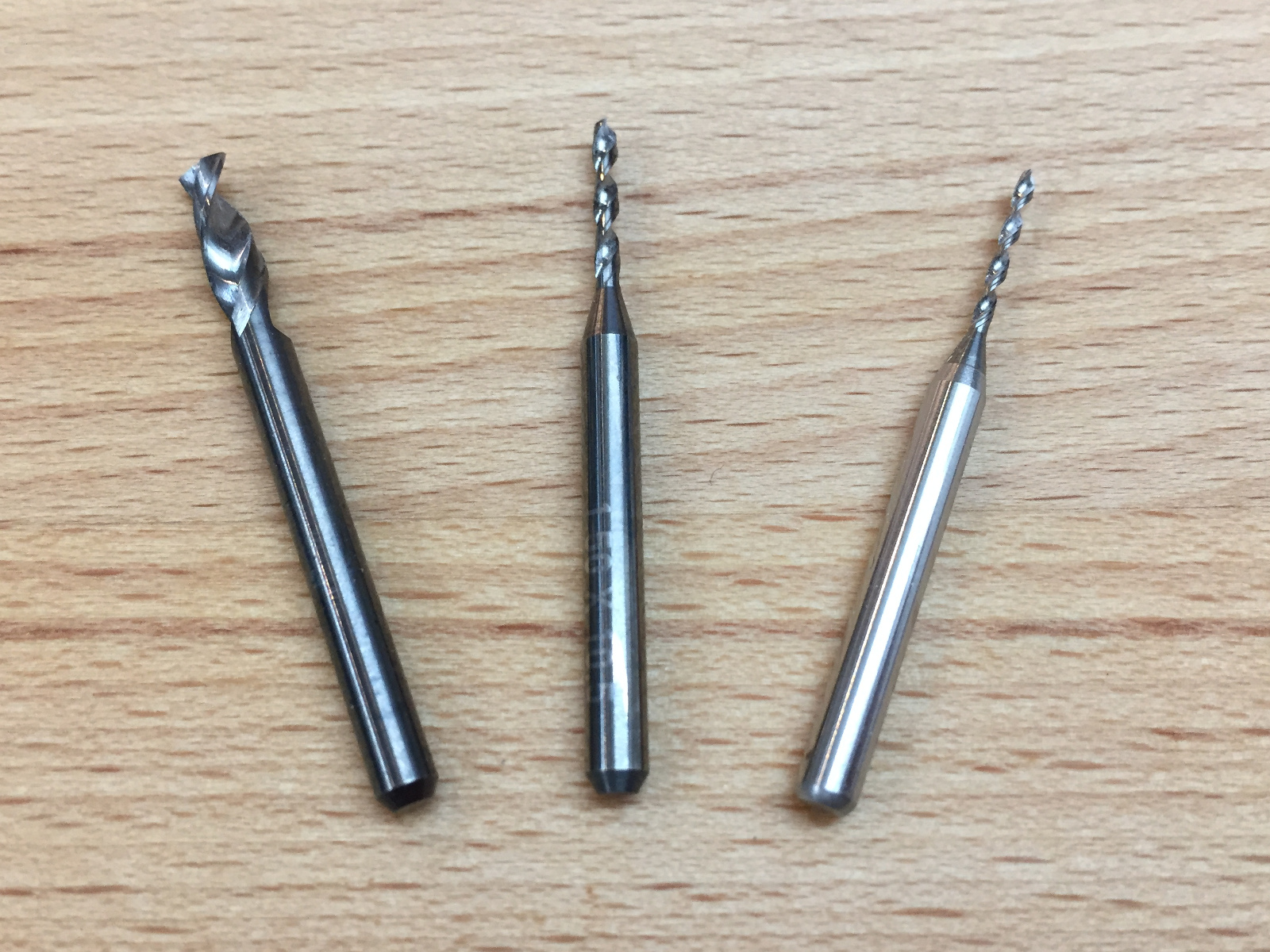
My favorite carbide drill bits: Ø3.2, Ø1.5 and Ø1.0 mm. (click to enlarge).
For drilling, don't use regular HSS (high speed steel) drill bits: the glass fiber in the FR-4 is extremely hard and will dull your tools after just a few holes. Use hard metal (tungsten carbide) bits instead: they will last for a long time, but are extremely fragile: use a steady drill press and wear safety glasses. Also wear a mask, because you don't want to breathe glass fiber dust.
For home purposes, I mainly use three different diameters: Ø1.0 mm for the majority of the components, Ø1.5 mm for the big leads of some heavy components (large electrolytic capacitors, fuse holders, terminal blocks,...) and Ø3.2 mm for the mounting holes.
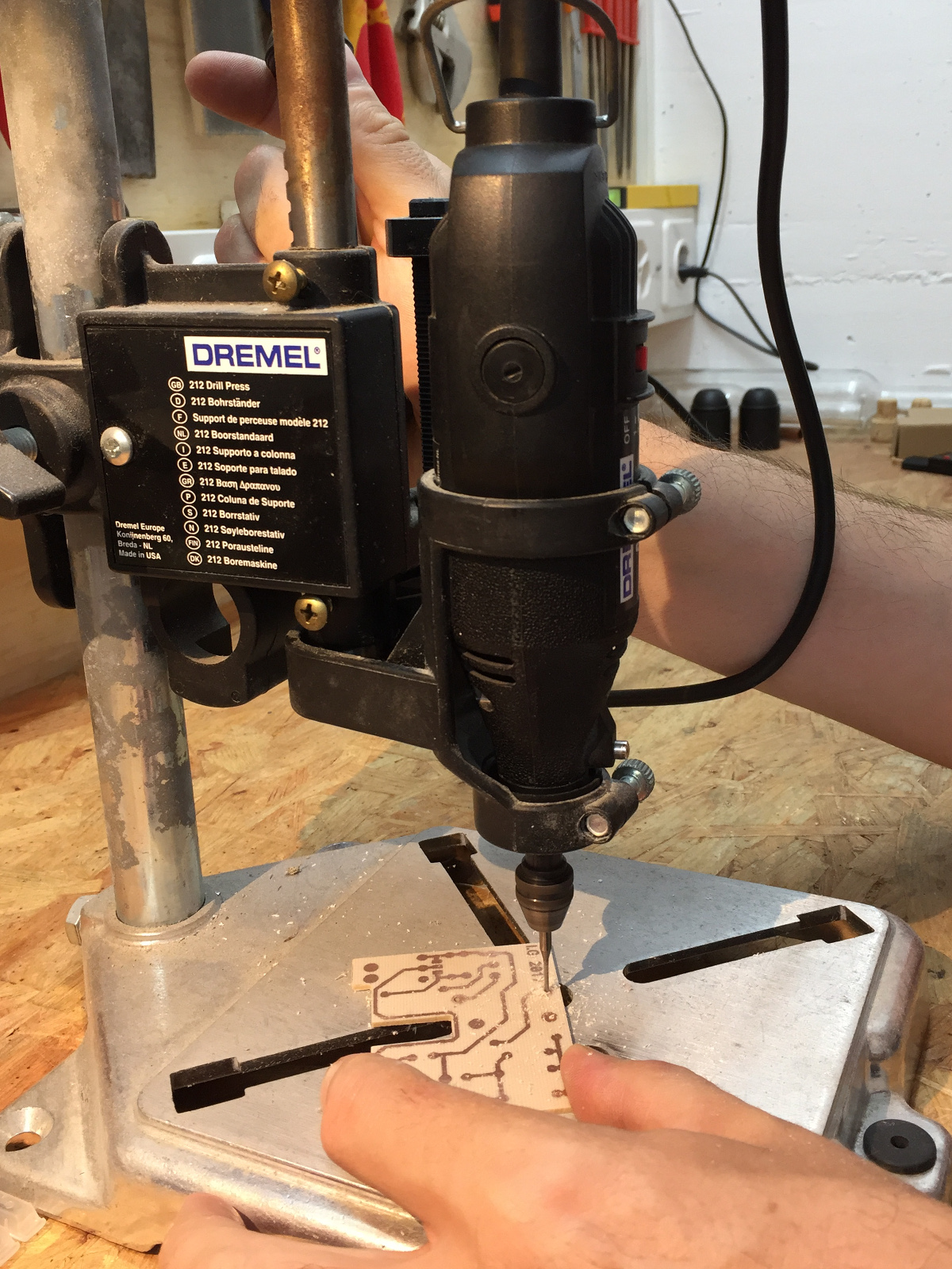
Drilling the PCB with a rotary drill mounted in a drill press jig.
Don't even think about drilling free-hand with a thin carbide bit, they break
like glass if bent. (click to enlarge).
For cutting PCBs, a hacksaw works quite well, and is spite of the hardness of the glass fiber, the blade lasts reasonably long. You can also file the edges with a regular metal file that also resists quite well to the hardness of the FR-4.
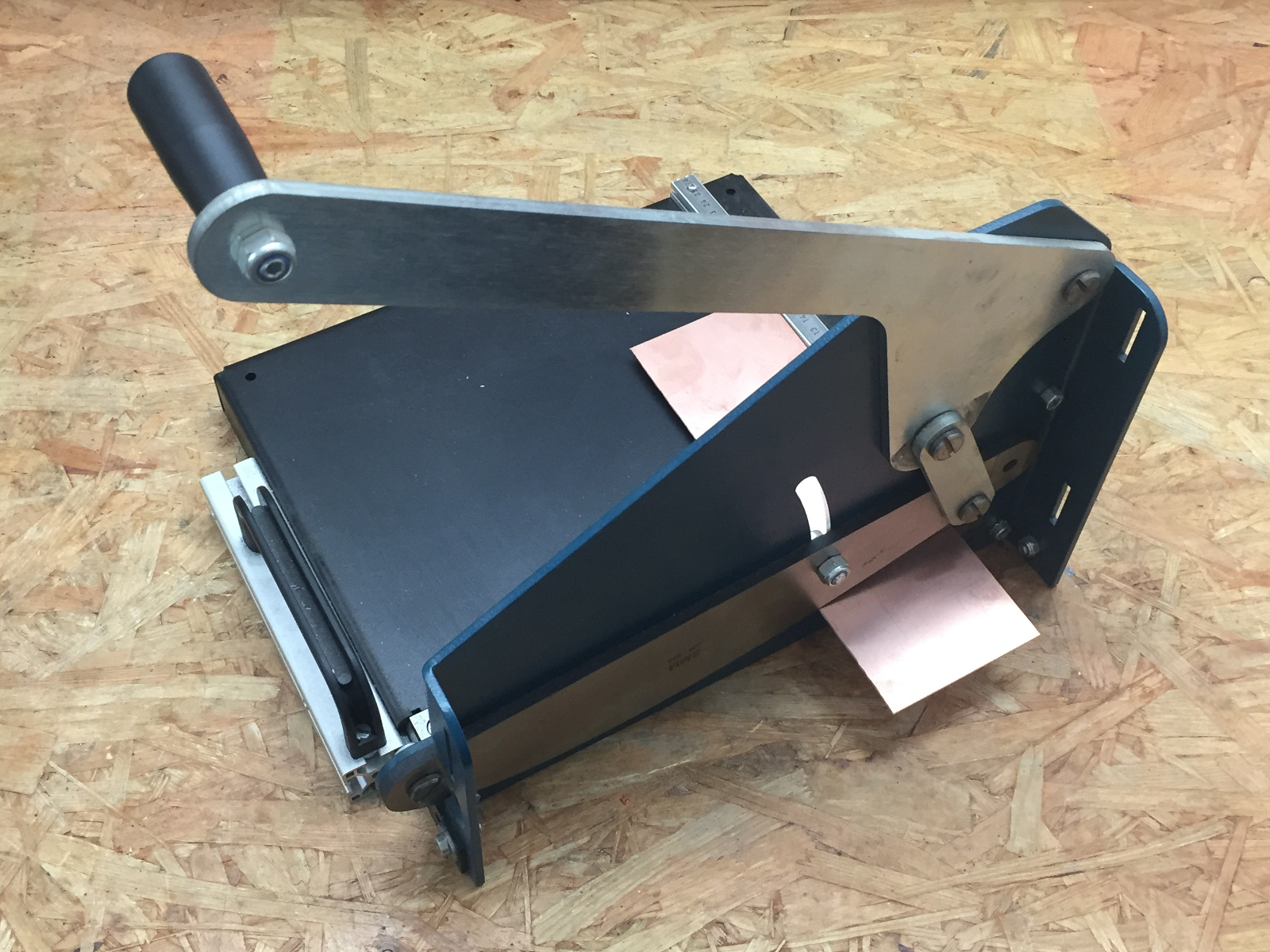
A guillotine cutting press for cutting PCBs is my preferred tool.
(click to enlarge).
But in my opinion, the best way to cut PCBs is a guillotine cutting press: it's expensive and it can only make straight cuts, but it generates no dust and makes good cuts in a blink of an eye. It's a really handy tool that saves you a lot of time. In spite of its price, if you often cut PCBs, it's definitely worth having one in your workshop. And you can use it to cut sheet metal as well.
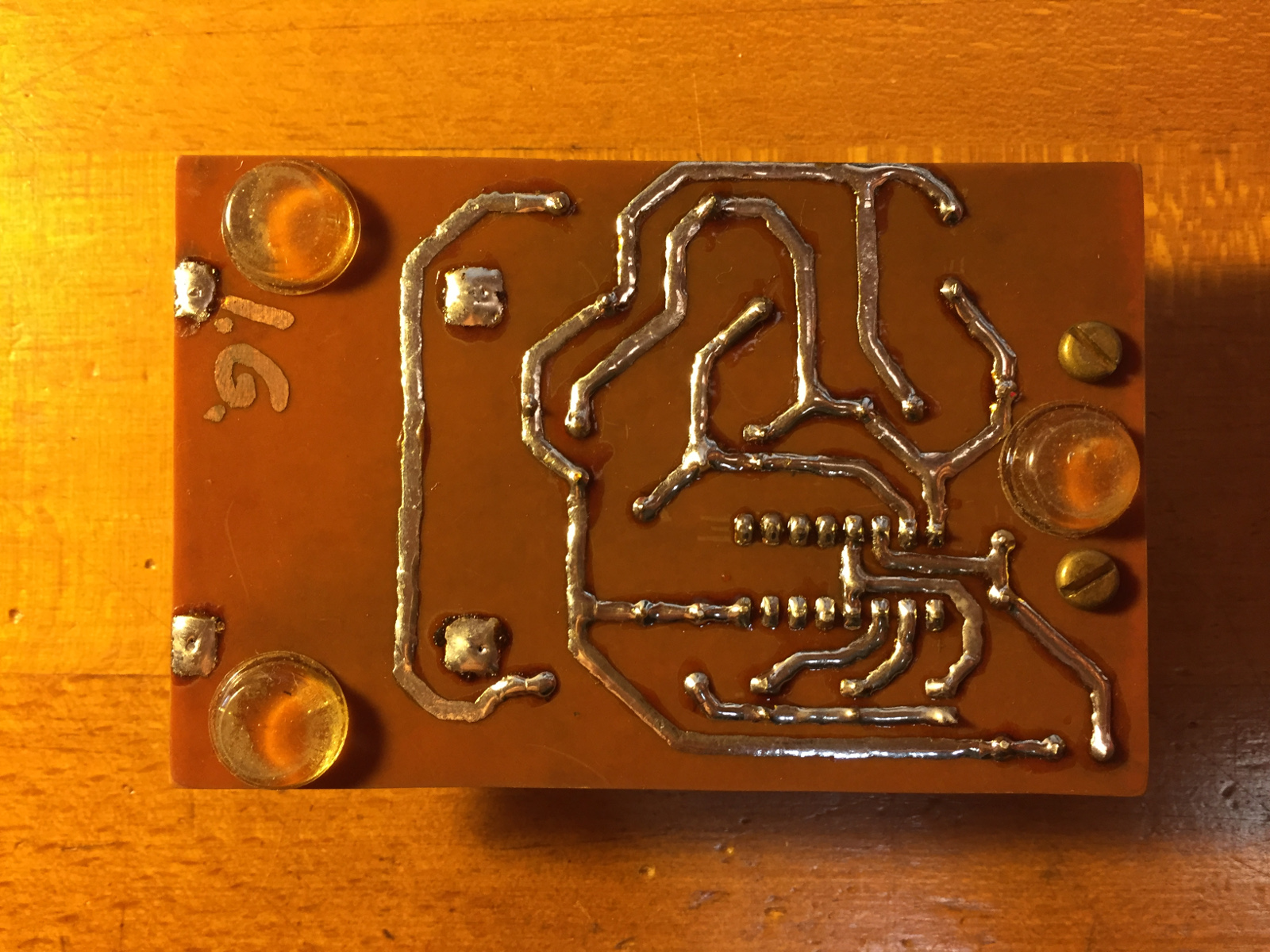
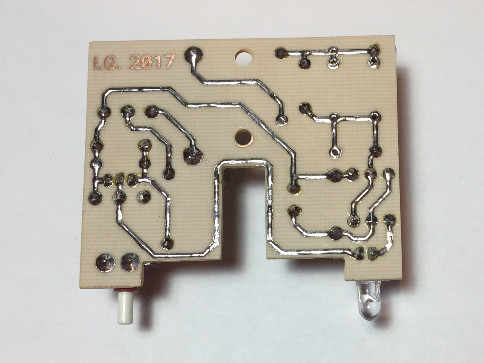
The finished PCB, ready for soldering. (click to enlarge).
And now we have it: a nice new PCB ready to be populated.
Some people like to tin the traces, so that they don't oxidize. This is not strictly necessary, but nice to have, especially if you plan to solder your PCB at a later time. You can use chemicals to do that and you can easily buy them online: they are called "cold tinning solutions". All you need to do is dipping your PCB in the solution for a few seconds and rinse it with water. I usually don't do it unless I have to solder fine pitch SMD comoponents. When I have time, for regular through-hole PCBs, I like to tin the traces with my soldering iron: it's by far the most inefficient way of doing it, but I like the look of the PCB. When I don't have time, I just leave the bare copper: for hand soldering, a little oxidation is not an issue, the flux in the solder will easily get rid of it in no time at all.
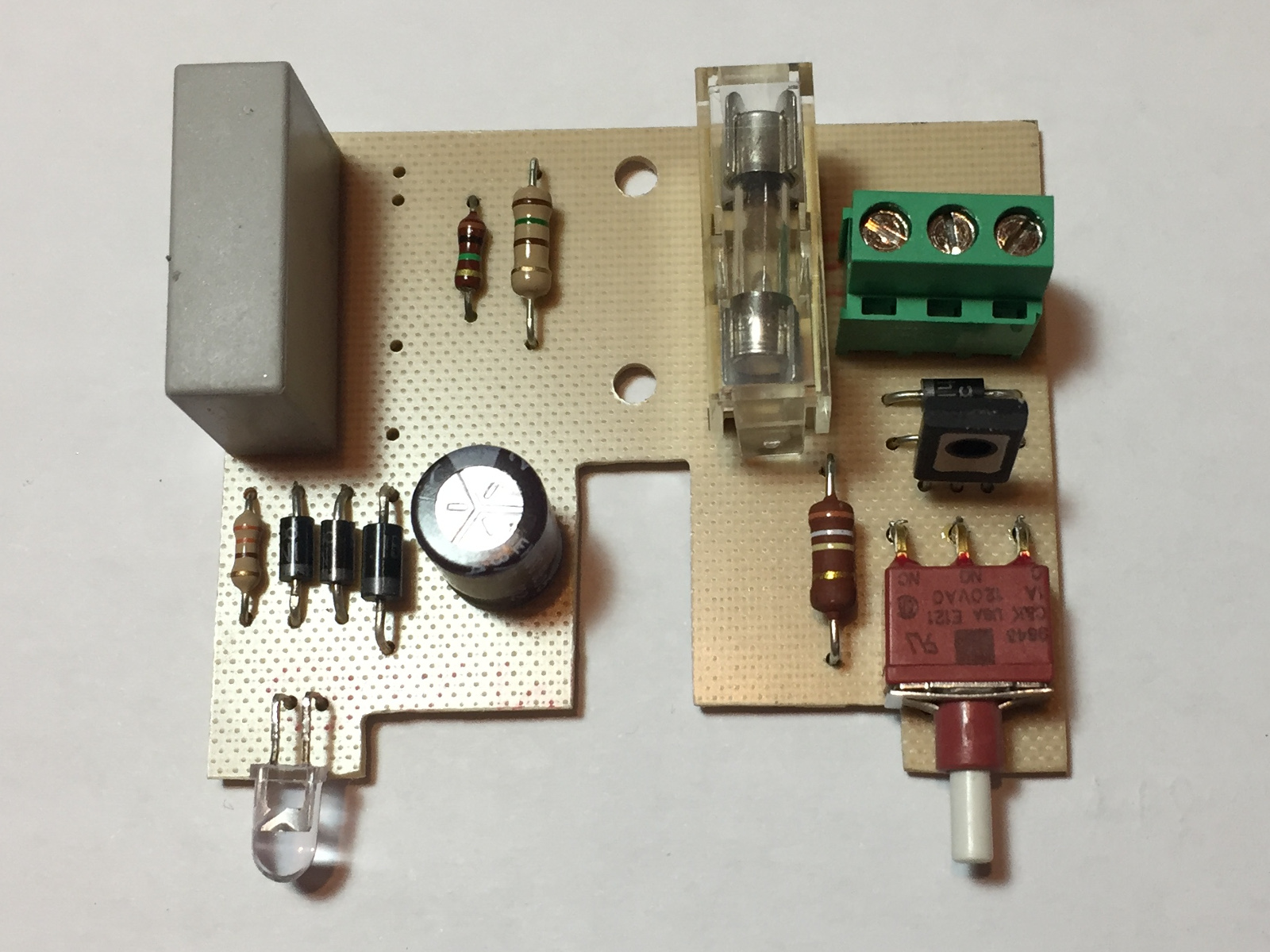
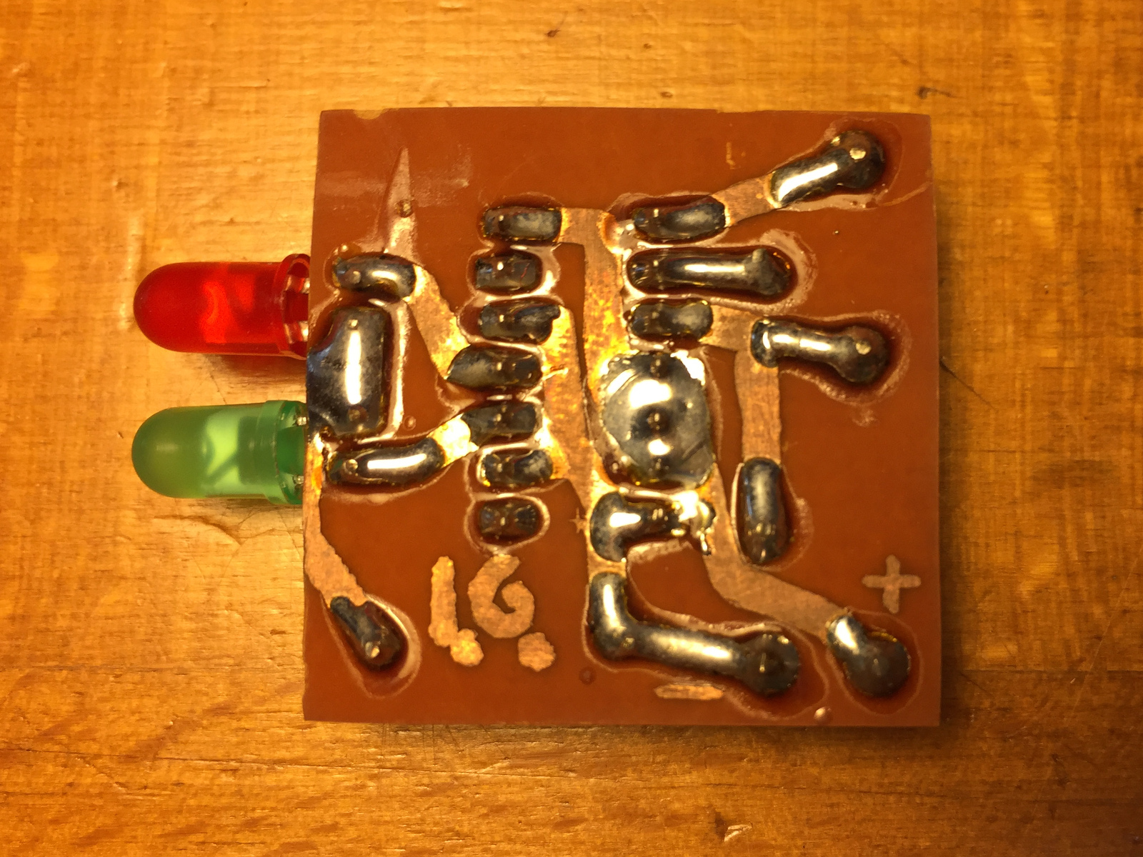
The finished fully assembled product viewed from both sides. (click to enlarge).
I've been making PCBs for my home projects since the mid '80s. It has always been a long and tedious process, one PCB required about half a day of work. Over the years, I looked for alternative methods that could speed up the process and that do not require expensive or hard to find materials. The two methods explained here, toner transfer and hydrochloric acid etching allow producing a PCB in less than half an hour, from the design to the ready to solder board. I personally like this way of making PCBs and use it quite often, much more often than before and I hope you find it useful as well.
| Home | Electronics | Page hits: 052230 | Created: 12.2017 | Last update: 12.2017 |